Why printed circuit board testing is needed
Testing electronics, especially PCBs, is therefore extremely important as it prevents many problems from occurring. To better understand how PCB testing can improve your products, learn more about too what PCB testing entails and what primary methods are used to evaluate PCBs.
PCB testing is necessary for several reasons
First, testing PCBs throughout the production cycle helps prevent problems and errors in the final production run. Identifying and correcting problems in the early stages of production is much more efficient and less expensive than repairing defective boards after they are finished.
Second, PCB testing allows you to minimize errors and problems during the manufacturing process itself. Design analysis techniques can be used in the early stages to identify potential problems that could affect the manufacturing process. This allows the necessary adjustments and optimizations to be made before the actual manufacturing process.
Third, PCB testing focuses on detecting short circuits, defective solder joints and board functionality. These tests are performed on prototype boards or small batches and ensure that each PCB that passes testing will function properly and meet requirements and expectations.
Overall, PCB testing is key to ensuring the quality and reliability of electronic products. It helps minimise the risk of defective boards, reduces repair costs and increases confidence in the product before it is released to the market.
Companies see PCB testing as a necessity because it provides many benefits.
The main advantages of testing printed circuit boards:
1. Fault Identification:PCB testing helps to identify problems in the PCB, whether they are functionality or manufacturability issues.
2. time saving: testing PCBs in the early stages enables time saving in the long run. With testing, designers can identify major issues during the prototyping phase and quickly fix them, reducing overall production time.
3. Cost reduction: PCB testing prevents the production of defective boards and reduces the costs associated with repairing them. Through prototyping and small-scale testing, production costs are minimized and the quality and reliability of the final product is ensured.
4. Reduced product returns: PCB testing reduces the risk of selling defective products or products that do not meet the required standards. This reduces costs associated with customer returns and handling of defective goods. Fewer product returns also increases customer satisfaction and improves the company's reputation.
5. Increased safety. Pre-manufacturing testing ensures that boards are safe and do not pose a risk to people's health and lives. It also prevents damage to equipment and injury to workers during the manufacturing process.
What is pcb testing and what is being tested?
Testing and inspection of printed circuit boards involves a wide range of methods used to verify compliance with printed circuit board standards. These standards focus on the proper function of the PCB in accordance with the project specifications and on detecting any defects. Electrical board testers and other test methods are used for this purpose.
Circuit board testing procedures perform analysis of several board components. These components are carefully examined to ensure their quality.
The main processes tested include:
Lamination: the quality of the lamination is crucial to the life of the PCB, as peeling of the laminate can cause problems with the ultimate functionality of the board. Lamination testing typically focuses on the laminate's resistance to peeling due to force or heat.
Copper plating and intermetallics: The copper foil on the circuit board is laminated to the board and provides its conductivity. The quality of the copper is often tested, through analysis of the tensile strength and elongation of the material.
Solderability: Testing the solderability of the material is important for the proper function of the circuit board, as it ensures that components can be soldered correctly to the board and prevents soldering defects in the final product. The most common tests are the ability of the surface to accept solder and how well the solder wets.
Hole wall quality: Hole wall quality is another important aspect of the circuit board that ensures that the hole walls do not crack and are not clogged with laminate. The quality of the hole walls is usually tested under cyclic loading and rapidly changing temperatures to see how well they resist thermal changes.
Electrical properties: electrical conductivity is essential for any printed circuit board, and therefore a common test is the ability of the printed circuit board to conduct electrical current with minimal leakage.
Moisture Absorption: Many circuit boards operate in high humidity environments, and therefore a common test is the moisture absorption of the circuit board. In these tests, the board is weighed before and after exposure to the humid environment, and significant weight changes could indicate board failure.
Cleanliness: PCB cleanliness refers to the ability of the PCB to withstand environmental factors such as corrosion and moisture. Typically, an analysis of the board is performed before and after exposure to various environmental conditions.
How to test printed circuit boards
There are several methods of testing printed circuit boards and none of them are universal and will catch all problems or meet every designer's requirements. When choosing a test method, it is important to carefully consider whether it meets the specific needs of your manufacturing environment. There are several factors to consider when making your selection, including the type of product being tested, the problems you want to test, and the reliability of the test method.
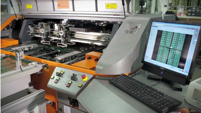
Optical Inspection
Also known as AOI (Automatic Optical Inspection), it is a process that visually inspects the quality of solder joints and the correct position and fit of components on a printed circuit board. Optical inspection can be performed with the naked eye, which is common in prototyping and small-scale manufacturing, or with automated systems that include moving cameras that capture details of the board with the components mounted. The automated system is trained to recognize properly seated and defective components and solder joints, and is able to identify errors such as defective soldering, missing components, short circuits, and other defects. The inspection results are displayed to the operator, who then verifies that the board is actually defective.
However, with optical inspection, the accessibility of the tested areas for visual inspection is important, so it is crucial to space the components appropriately with sufficient gaps when designing the PCB. Component spacing is one of the optional design rules that can be checked during design. Another option for detecting defects is not only from the top view, but also from an inclined view or by using an endoscopic view from the side of the component housing. This provides more detailed information about the condition of the mounted components and solder joints.
The AOI method can reveal:
- absence of components
- incorrect components in a given position
- displacement or rotation of components
- component rotation or incorrect polarity
- short circuit
- foreign object on the board
- unconnected pin
- lifted pin
- incorrectly soldered THT pin
- different height of individual BGA corners
FCT functional testing
This method is often used when testing lower cost products or as part of a final inspection. In this test, the product is tested as a whole without detailed inspection of the internal signals. The tester uses special jumper cables to feed excitation signals to the product inputs and checks the response at the outputs. If the device is equipped with programmable components, test firmware is usually loaded into them to facilitate fault detection. This type of testing usually requires operator interaction. In more advanced testers, operators are replaced by robots and specialized automated systems. These automated systems check mechanical parts and indicating elements such as LEDs, displays, audible alarms, buttons, etc.
This method of testing reveals them:
- functionality as specified
Functional testing is particularly suitable for smaller scale and small batch production because the cost of a functional tester is relatively low. However, it is important to consider how to output important signals to the connector. There may be compromises in this method when simulating electromechanical components or when checking displays with a camera, etc.
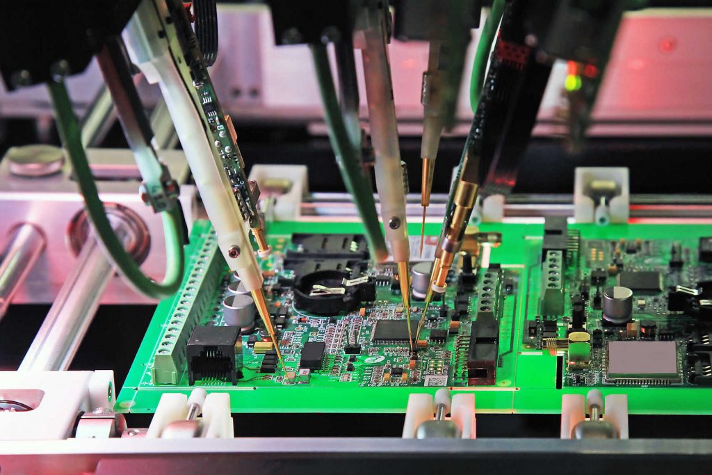
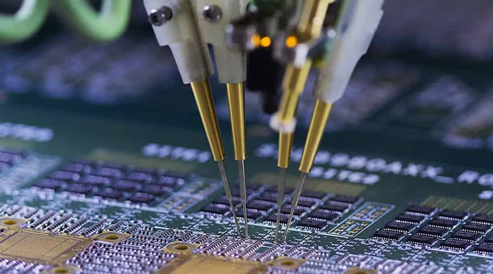
ICT Testing
The In-Circuit Testing (ICT) method is a widely used method for testing electronic devices after PCB assembly. It can electrically measure the presence and static values of components. The principle of In-Circuit Electrical Test is to measure signals directly on the printed circuit board. The system generates excitation signals and then checks whether the circuit response is correct. Special test needle contacts that are connected to the product to be measured are used for testing. Each circuit board that is tested by this method must contain 'testpoints' or test points, usually located on the underside of the board.
This shows that it is necessary to prepare the product for this type of testing during board development. The board must be designed so that each test point on the board can be reliably and repeatably connected using test needles.
The design of the test points on the board must meet not only the basic rules for PCB design, but also the technological requirements for manufacturing, mounting and soldering. The test needles themselves are special products that ensure flexible contact with the board.
The top of the needles have sharp edges or tips that remove the surface layer of dirt on the solder joint and provide a small transient resistance for the current that passes through them during the test. The test area on the board should match the size and finish of the needle.
This method can be used to:
- check for the presence of components
- check the orientation of the components
- test the correct value of passive components
- detect short circuits
- detect disconnections caused by incorrect soldering of components
- measure basic circuit quantities and evaluate whether the PCB has been fitted correctly
Another important part is to create a combination or sequence of test signals for a specific board. The number of testpoints alone does not guarantee a successful test. Often, a set of independent (orthogonal) excitation signals, such as a "wandering one" or ripple injection into an analog network, is created and tested to see if this signal reaches the correct location and level. Testing of fully assembled PCBs, with testing of passive component values and their tolerances, short circuits, and most importantly, functional checks, is done via a contact needle array.
In the context of needle testing, mention should be made of the JTAG interface – automated integrated circuit testing. The two primary methods, automated optical inspection (AOI) and automated X-ray inspection (AXI), are the precursors to this solution for detecting faults at the beginning of production.
JTAG (Joint Test Action Group)
Testing a board with many paths required something like a bed of needles. As pin density increased and as the move to ball-grid-array (BGA) packaging was made, a new method of testing was required.
And so, in 1980, scanning was developed and standardized, and the technology became known to developers and engineers as JTAG.
The basic idea behind this technique is precisely the replacement of an array of pins with integrated electronic "pins"- cells that are implemented in an integrated circuit by separating its logic core from its physical pins. These thus act as "virtual" probes inside the component.
The individual cells are interconnected and controlled by logic implemented on the chip of the IC together with JTAG functional logic. This allows the application of serial loading of external test vectors simulating the values of input and output pins and then obtaining the resulting values. The operation of the input and output cells is controlled by four or five TAP wires.
The JTAG connection test verifies that the connections around the JTAG-enabled devices on the board are the same as those specified in the design.
In direct mode, this system can find the following faults on an assembled board:
- Short circuit between directly testable connections
- Short circuit of testable connections to power (log.1) or to ground (log.0).
- Interruption of testable connections
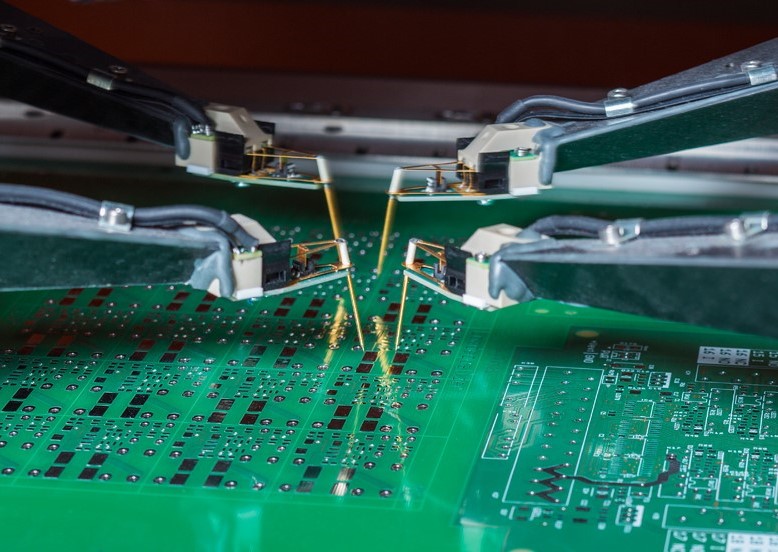
FPT - Flying probe testing
Flying Probe is electrical testing and currently the most flexible method of PCB testing for prototype production. It is based on a similar principle to ICT.
Literally flying probe is an alternative testing method for verifying the integrity of an assembled PCB, however this system differs from previous ICT testing in that instead of a fixed test fixture, only a few probes are placed around each test point on the board, there can be 2-8 probes with a needle. The flying probe system is easy to install and affordable, not requiring expensive test fixtures. In addition, any changes to the board that require modifications to the test system can be easily reprogrammed.
The disadvantage of FPT is that it is slow. While ICT can instantly test almost all points on the board, the FTP system must maneuver each probe to a single test point. However, for prototypes or small batch production, using Flying Probe testing can be very beneficial.
Gatema PCB Inc. as one of Europe's top prototype PCB manufacturers, uses state-of-the-art ATG A5 to ATG A7 eight-needle probe Flying Probe Testing equipment for electrical testing of unmounted PCBs.
Industry 4.0 brings intelligent testing to electrical engineering
The principles of Industry 4.0 are gradually making their way into all industries, including electrical engineering. Test-it-off, or the method of automated inspection of PCBs and products using a robotic system that combines multiple inspection methods at once, fits right into this principle. This system enables communication between different production nodes and can respond smoothly to any changes or inspection requirements.
Test-it-off uses an intelligent robotic system that is responsible for automating the PCB testing process, bringing objectivity to the testing process while generating accurate statistics on the status of production.
Thanks to Industry 4.0 principles and communication between production nodes, Test-it-off is able to react quickly to changes in the production environment. For example, if board specifications change or new requirements emerge, the system automatically adapts and starts to perform the appropriate tests. This ensures flexibility and efficiency in the production process.
An important part of Test-it-off is also the collection of data and the generation of statistics on the status of production. In this way, the performance of the production process can be monitored and analysed, any shortcomings can be identified and the necessary improvements can be made.
Overall, the Test-it-off system brings the benefits and innovations associated with Industry 4.0 principles to the electrical industry. Thanks to the communication between production nodes and the intelligent robotic system, flexibility, objectivity and efficiency in the PCB testing process are ensured, contributing to an improved production environment and quality of the final products.
Connect with our specialists