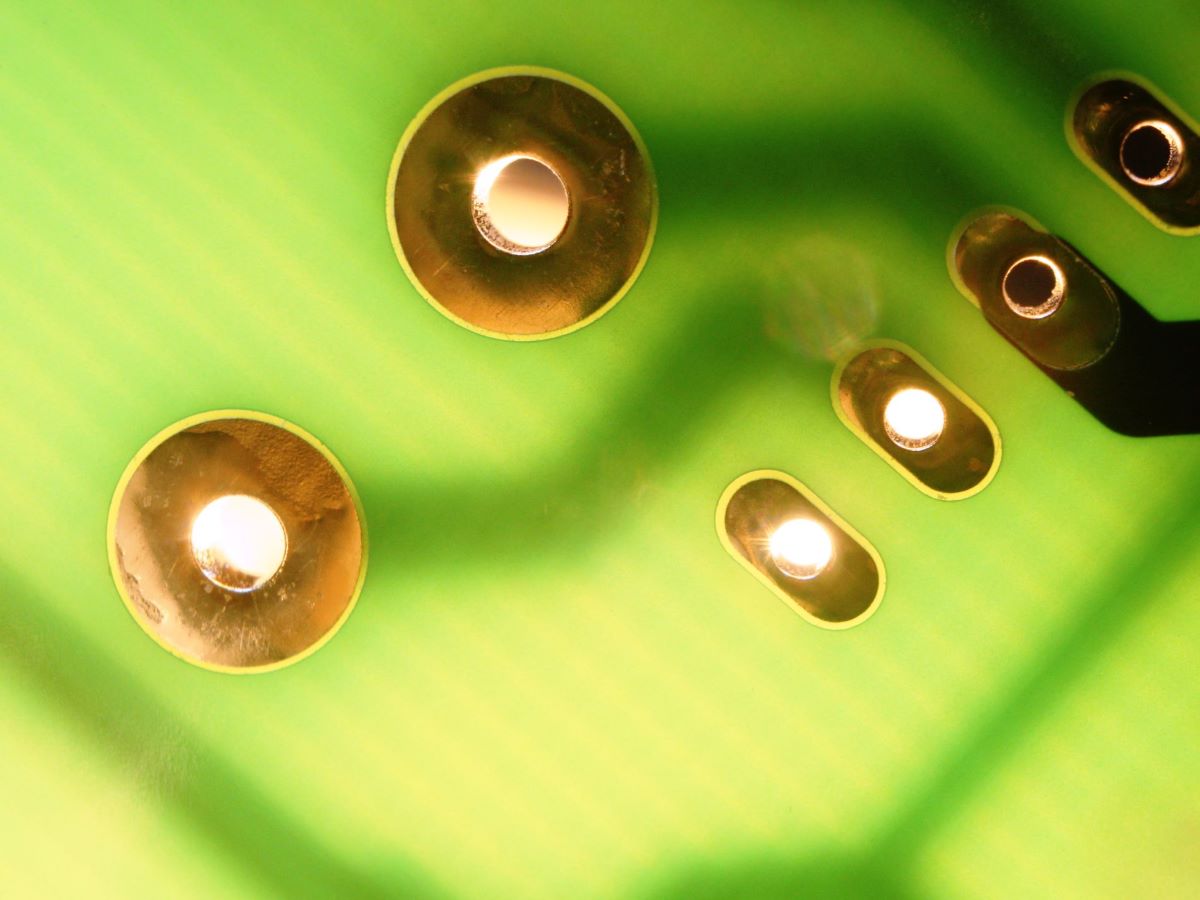
Microvias in printed circuit boards
Comparison of "stacked" and "staggered" microvias
Stacked Microvias
Stacked microvias are a special type of microvias that combine multiple through-hole microvias to increase connection density on the PCB. This allows for greater flexibility and space optimization, which is ideal for devices with high demands for miniaturization.
Advantages of Stacked Microvias
Increased Connection Density: Stacked microvias enable more connections in a smaller space, leading to more compact PCB designs.
Space Optimization: By placing multiple microvias in the same location, space on the PCB can be utilized more efficiently.
Design Flexibility: Stacked microvias offer greater design options for the PCB, which is crucial for complex industrial applications.
Challenges in Using Stacked Microvias
Design Complexity: Multilayer structures require more careful planning and simulations to ensure proper functionality and reliability.
Technological Limitations: Manufacturing stacked microvias may require special technologies and procedures, which can affect production costs and time.
By using stacked microvias, it is possible to achieve high connection density and optimize space on the PCB, which is particularly valuable for applications with high demands for miniaturization and performance.
Staggered Microvias
Staggered microvias are another specific type of microvias that are placed to be spaced or offset from each other. This design can be advantageous for certain applications and can offer several key benefits.
Advantages of Staggered Microvias
Signal Noise Reduction: Staggered microvias can help minimize electrical noise between different signal paths, significantly improving the performance and reliability of the PCB.
Space Optimization: This design allows for more efficient use of space on the PCB, which is valuable for compact designs and applications with limited space.
Greater Design Flexibility: Staggered microvia provides greater flexibility in arranging connections and components, which can be advantageous for complex designs.
Challenges in Using Staggered Microvias
Complex Design: Designing and planning staggered microvias can be more complex than traditional microvias, requiring careful planning and simulations.
Production Requirements: Staggered microvias may require special manufacturing technologies and procedures, which can affect production costs and time.
Staggered microvias offer additional design options and can be beneficial for certain applications, especially where minimizing electrical noise and optimizing PCB performance are necessary.
Where Microvias Find Applications
Microvia technology remains a major trend in the PCB industry, with expected further growth in the coming years. Benefits such as higher packing density, improved electrical performance, and enhanced thermal performance make them an ideal choice for a wide range of applications. With the advent of 5G and the internet of Things (IoT), demand for microvia PCBs is expected to significantly increase, opening up new possibilities in industrial design.
Telecommunications:
High-speed data communication in telecommunications requires the use of microvias to maintain signal integrity and performance.
Space:
In the aerospace industry, microvias are used for component miniaturization and reducing weight and space in satellites and spacecraft.
Medicine:
In the healthcare industry, microvias are crucial for enhancing the performance and functionality of medical and technological devices such as implants and wearable diagnostic equipment.
Reliability of Microvias
Microvias can improve PCB reliability by enhancing thermal performance and improving electrical properties due to lower inductance and capacitance. These improvements are key to ensuring signal integrity and optimal performance across a wide range of applications.
Potential Issues with Microvias
Despite their advantages, microvias also present some challenges, such as increased design complexity, manufacturing difficulties due to smaller constructions, and issues with inspection and testing due to reduced joint sizes.
Recently, concerns have arisen regarding the long-term reliability of microvias, particularly in "stacked microvias" configurations. These holes placed concentrically above each other exhibit susceptibility to failure, raising questions about their long-term reliability.
Although "staggered microvias" offer better reliability, this approach often requires more space, which can be problematic in applications with limited space. Researchers are focusing on identifying the causes of these failures and searching for optimal microvia structures to increase their reliability. Advanced microscopic techniques, such as Scanning Electron Microscopy (SEM), Focused Ion Beam (FIB) microscopy, and Scanning Tunneling Microscopy (STM), are used for this research. These methods provide a detailed view of the microstructural characteristics of the holes, but their interpretation requires caution to avoid distorting the results.
Conclusion
Caution in interpreting data and analyzing "microvia holes" using verified methods are crucial for understanding and improving the reliability of modern PCBs. Despite the complexity and challenges associated with this research, it is clear that careful analysis and innovative approaches will allow us to overcome these obstacles and achieve higher performance and resilience in future designs.
Connect with our specialists