The history and evolution of PCB - printed circuit board designs
Origins and Early Development
In 1903, one of the famous German inventors, Albert Hanson, filed a British patent for a device described as a flat foil conductor on a multi-layer insulating board. In the early 20th century, American inventor Charles Ducas pioneered the concept of "printed wiring", laying down electronic paths on insulated surfaces. However, it was Austrian engineer Paul Eisler who made significant progress in PCB development during World War II. Eisler's invention of a PCB-equipped radio tube paved the way for the mass production of proximity fuse circuits, vital for military operations.
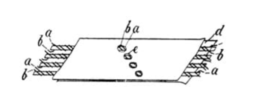
The first patent drawing by Albert Hanson
The 1960s: Revolutionizing PCB Development with Integrated Circuits
The 1960s marked a turning point in PCB development with the introduction of integrated circuits (ICs). This breakthrough allowed for the integration of multiple components onto a single chip, ushering in the era of multi-layer PCBs. With ICs, circuit density increased, enabling greater miniaturization and paving the way for more sophisticated electronic devices.
The 1980s: Embracing Surface-Mount Technology and Material Advancements
In the 1980s, surface-mount technology (SMT) emerged, streamlining assembly processes and enhancing circuit performance while reducing manufacturing costs. Simultaneously, advancements in materials expanded the scope of PCB applications. Traditional substrates like glass epoxy and paper phenolic gave way to modern options such as polyimide and acrylic.
The 1990s: Further Innovations in PCB Technology
The 1990s witnessed significant advancements in PCB technology, including the introduction of ball-grid array (BGA) IC packaging, which expanded PCB functionality. Design for testability guidelines emerged to ensure PCB quality, contributing to the industry's rapid growth. Microvias were introduced to accommodate high-density PCB designs, leading to the widespread use of flexible PCBs in motion-based applications.
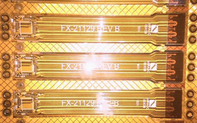
Flex-rigid boards
The Turn of the Millennium: Addressing Emerging Trends and Challenges
As the new millennium approached, PCBs continued to evolve to meet emerging trends and challenges. Bio-degradable materials were explored as alternatives to traditional substrates, addressing environmental concerns associated with electronic waste. Additionally, advancements in areas such as virtual reality (VR) and augmented reality (AR) drove the demand for flexible PCB designs capable of fitting into irregular shapes, further pushing the boundaries of PCB innovation.
Conclusion
The evolution of PCBs from their humble beginnings to their current state reflects the dynamic nature of the electronics industry. As technological advancements continue to shape the landscape of modern technology, PCBs remain at the forefront, enabling the development of innovative solutions that push the boundaries of what is possible. With a rich history of adaptation and innovation, PCBs are poised to play a key role in shaping the future of technology for years to come.
Connect with our specialists