BGA Package and Its Use in Electronics Manufacturing
What is BGA?
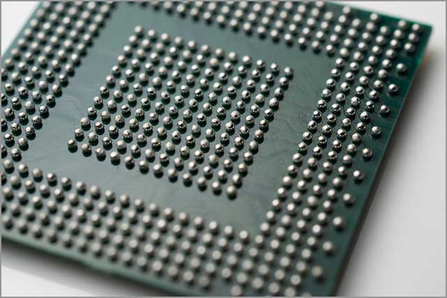
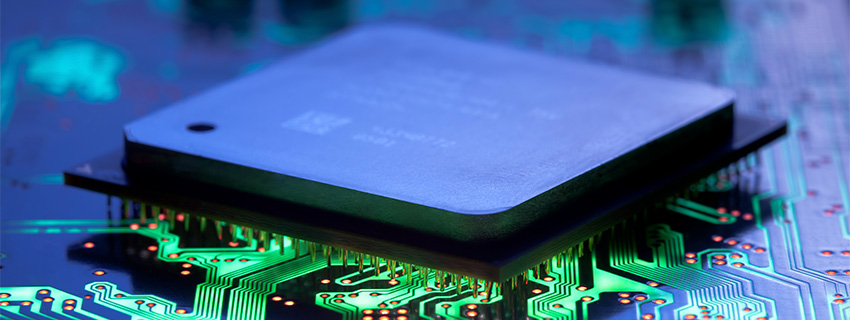
BGA (Ball Grid Array) belongs to the SMT (Surface Mount Technology) packages, which are packages with surface mount assembly. BGA is one of the encapsulation methods used for connecting components in integrated circuits. It is a type of package where the leads do not pass through the printed circuit board but are mounted only on the surface of the component side of the PCB. Therefore, it is evident that connections to such integrated circuits can only be made from the bottom side, not from the sides. The connection points, in the form of a ball grid array, are located on the bottom side of the package. These balls are connected to corresponding contact pads on the PCB.
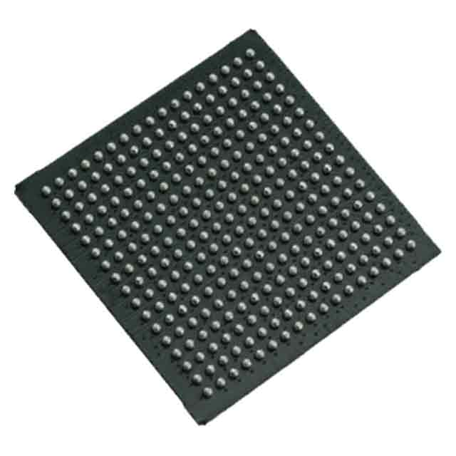
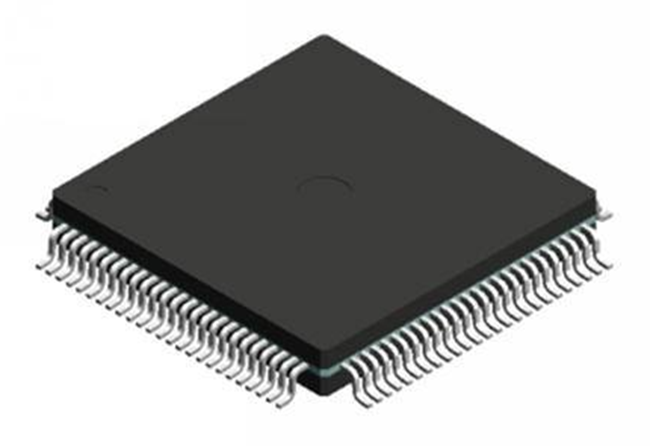
BGA with its bottom-ball grid arrangement of connectors is more advantageous than, for example, the QFP (Quad Flat Pack) package, which has connectors on the sides of the package. Side-mounted connectors mean that there is limited space for pins, which must be close to each other and significantly reduced in size to provide the necessary amount of communication. BGA utilizes the bottom side of the package where there is ample space available for connections.
Reasons for using BGA:
There are several reasons why Ball Grid Array (BGA) packages are used in the design and manufacturing of computer components and other high-performance electronic devices:
- Increased interconnect density:
BGA allows for higher interconnect density on the printed circuit board (PCB). The arrangement of balls on the bottom side of the package enables the integration of more terminals compared to other package types, such as Single In-line Packages (SIPs). This allows for more complex circuitry to be accommodated on a smaller PCB footprint.
- Enhanced thermal conductivity:
BGA packages have better thermal conductivity compared to other package types. The balls, directly connected to the PCB, facilitate uniform heat distribution and transfer into the board. This helps dissipate heat and maintains lower temperatures for the integrated circuit, which is crucial for its reliability and longevity.
- Improved mechanical reliability:
BGA packages provide better mechanical stability compared to other package types. The balls on the bottom side of the package create numerous interconnections with the PCB, increasing strength and resistance to vibrations and mechanical stress. This is particularly important for mobile devices and products subjected to movement or shocks.
- Electromagnetic compatibility (EMC):
BGA packages, with their short interconnections and compact ball arrangement, reduce inductance and electromagnetic interference. This is advantageous for devices operating at higher frequencies, minimizing signal interference and ensuring proper device functionality.
- Ease of automation: BGA packages can be relatively easily assembled and soldered using automated manufacturing processes. The ball arrangement allows for the use of Surface Mount Technology (SMT) placement machines, which are widely available on production lines.
Overall, BGA packages offer advantages in terms of interconnect density, thermal management, mechanical reliability, electromagnetic compatibility, and ease of automation in the manufacturing process.
Different Types of BGA
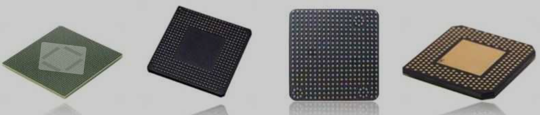
BGA packages come in various types, each with its specific characteristics and applications. Some common types of BGA packages include:
- Full BGA: Full BGA packages have balls distributed across the entire bottom surface of the package. These balls directly connect to the contact pads on the PCB, allowing for higher interconnect density.

- Array BGA (ABGA): Array BGA packages have balls arranged in a regular matrix on the bottom side of the package. This type of BGA is often used for integrated circuits with a high number of terminals, requiring a stable and precise interconnect arrangement.
- Micro BGA: Micro BGA packages are smaller variants of BGA packages used in very compact electronic devices. These packages typically have smaller ball diameters and dimensions, enabling the production of devices with a lower profile.
- Stacked BGA: Stacked BGA packages have a layered structure, where integrated circuits are placed in stacked layers. Pins or balls are present only on the bottom side, which is directly attached to the PCB. The upper layer is connected to the lower layer through internal signal and power connections.
- Package on Package (PoP): Package on Package is a technology that allows stacking two or more integrated circuits on top of each other as separate packages. The lower integrated circuit (bottom package) is directly attached to the PCB, while the upper one (top package) is placed on top of the lower integrated circuit and connected using solder balls or other interconnects. This method enables higher integration density and reduces the overall device size. PoP is commonly used in mobile devices such as smartphones and tablets, where high integration density and compactness are required.
- Flip Chip BGA: Flip Chip BGA packages have the integrated circuit directly connected to the package using solder balls. This design allows for better thermal conductivity and electrical performance and is often used in applications requiring high signal speed and reliability. The main advantage lies in shorter electrical paths compared to other types of BGA packages. The tin-lead ratio in this type of BGA is typically 63:37.
- PbBGA: PbBGA is a type of BGA package that contains lead (Pb) in the solder paste or balls for connection. This type of BGA was common before the introduction of RoHS lead-free directives that restrict the use of lead in the manufacturing process.
- Lead-free BGA (LFBGA): LFBGA is a BGA package that is either lead-free or contains minimal amounts of lead in compliance with RoHS directives. LFBGA packages utilize alternative lead-free solder alloys, such as tin-silver-copper alloys.
- Ceramic BGA (CBGA): CBGA is a BGA package made of ceramic material. Ceramic packages have excellent thermal conductivity and mechanical strength, making them advantageous for high-performance and heat-intensive applications.
- Organic BGA (OBGA): OBGA is made of organic material, typically epoxy resin. Organic packages are often used for cost-effective applications but are less thermally efficient compared to ceramic packages.
- Flex BGA (FBGA): FBGA is a type of BGA package mounted on an elastic substrate, such as a flexible film or substrate. These packages are suitable for applications where flexibility needs to be maintained, such as flexible electronic circuits.
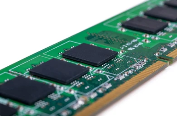
- Plastic Ball Grid Array (PBGA): PBGA is a type of plastic integrated circuit package that features ball interconnects on the bottom side. PBGA packages are widely used in the electronics industry due to their reliability, ease of assembly, and low cost. They are commonly used in mobile devices, computers, consumer electronics, and other surface-mount applications.
Advantages of BGA
Higher pin density:
One of the biggest advantages of BGA packages is their ability to provide a higher pin density. By arranging ball grid arrays on the underside of the package, more pins can be placed in a smaller area. This means that a greater number of functions can be integrated.
Improved electrical properties:
BGA packages also offer better electrical properties compared to other packages. The short and evenly distributed ball grid arrays result in lower inductance and smaller parasitic capacitance. This brings the advantage of reduced noise, improved signal integrity, and decreased signal interference risk. The improved electrical properties of BGA packages allow for higher data transfer speeds and enhance overall device performance.
Enhanced thermal properties:
The ball grid arrays on the underside of the package serve as excellent channels for heat transfer from the circuits to the PCB (printed circuit board). This helps dissipate heat from the chip and ensures efficient heat dissipation.
Simplified automated manufacturing:
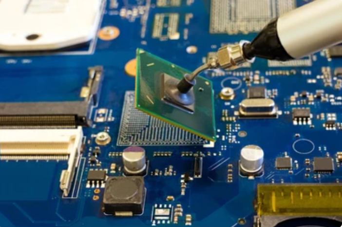
Another advantage of BGA packages is their easy compatibility with automated assembly processes. Using reflow soldering, BGA packages can be easily and precisely placed and connected to the PCB. The precise arrangement of the solder balls allows for high soldering accuracy.
Smaller size and weight:
Due to their higher integration density and compact design, BGA packages offer the possibility of creating smaller and lighter electronic devices. This is particularly important for mobile devices that require reduced weight while maintaining high functionality.
Disadvantages of BGA
Just like any other electronic package, BGA has its own set of disadvantages. These include the fact that BGAs are more susceptible to stress due to flexural tension from the circuit board, which can lead to potential reliability issues. Additionally, inspecting solder balls and soldered joints in case of faults is very challenging, especially when BGAs are soldered onto the printed circuit board. When considering the use of BGA technology, it is important to weigh these drawbacks and evaluate whether they are acceptable in relation to the specific project and desired goals.
Closing Statement
These are just a few examples of BGA (Ball Grid Array) surface-mount package types. There are many other specific types of BGAs available, varying in shape, size, ball pitch, and other characteristics. Choosing the right package type depends on the specific application, pin count, board size, and other factors.
You would likely agree that BGA packages offer a range of advantages that enhance the performance, reliability, and efficiency of electronic devices. Their higher pin density, improved electrical properties, enhanced thermal characteristics, easy automated manufacturing, and smaller size and weight make them an attractive choice for many applications in the electronics industry. BGA technology will continue to innovate and adapt to the specific needs of different sectors. For instance, in the fields of artificial intelligence, Industry 4.0, autonomous vehicles, or IoT (Internet of Things), high-performance BGA components with low power consumption and resilience to extreme conditions will be required.
Overall, it is expected that BGA technology will continue to play a crucial role in the electronics industry and contribute to the development of more powerful, smaller, and smarter devices.
Connect with our specialists