The production of PCB is often hampered by minor details. Keep an eye on it.
At the same time, however, he also points to the limits associated with automation of input into the system. “We are trying to make sure that the customers have the simplest possible input into production. To make most boards work in the way that customers enter them directly into the configurator on the website and we just check the things over. Unfortunately, there are still small limits in that regard that we are trying to eliminate. And they are both on the technology side where the individual programs do not communicate perfectly among themselves, or machine reading does not work perfectly, and on the side of people who constantly make small mistakes when entering,” adds Radim Vítek.
What mistakes can slow down the smooth preparation of the board for production? Often these are just little things.
- The data do not have the same zero point. They are not at the zero point or are mirrored in some way. The ideal zero point is such that is in the lower left corner, without mirroring, and preferably from a top perspective.
- Sometimes there is no indication of layer orientation. The ideal is to have a text in the data. If you mark a data file as pcb.top, you do not know whether the other person is looking from the bottom view or the top view, the readability of the text in the data will help with the orientation.
- Identification of copper layers, conventionally 1, 2, 3…, is sometimes missing in the data. This small thing is important for multilayer boards.
- Working with vector font in Eagle.
- Data that are exported from the design systems should have a clear structure, Pad, Line, Polygon. It happens that data come to us that are only from a polygon or crosshatched and cannot be easily converted.
- Drilled holes in negative inner layers are half in insulation and half in copper. The system then fails to discern whether they are to be connected to a layer or vice versa.
- Some “thermal pads” do not correspond to the design class - they may disappear during the manufacture. Ideally, therefore, the thermal pad should be enlarged according to the design class.
- The thickness of the text must also correspond to the design class. It happens that the texts on the board are 20 to 50 microns and then it is necessary to correct them. If you want a text in a solderless mask, 100 microns is the minimum for immersion gold. When applying Hot Air Levelling, it must even have 250 microns.
- If there is a chamfered edge of a gold-plated connector on the board, pay attention to the inner layers under the connector, which must be insulated as far as possible - ideally between 2 and 5 millimetres.
- Optimization for non-plated openings and pads exists. But a non-plated opening should not be on copper.
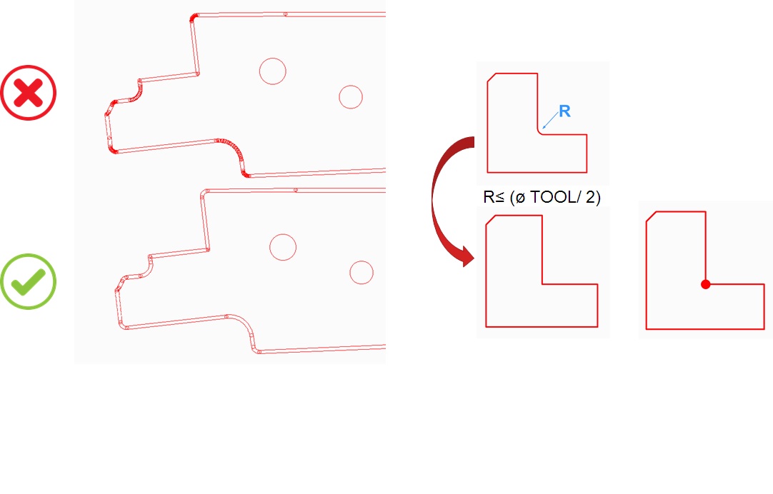
- Creating a milling program takes the most time during the preparation. Therefore, we recommend that the board outline contains only “arc” and “line”.
Connect with our specialists