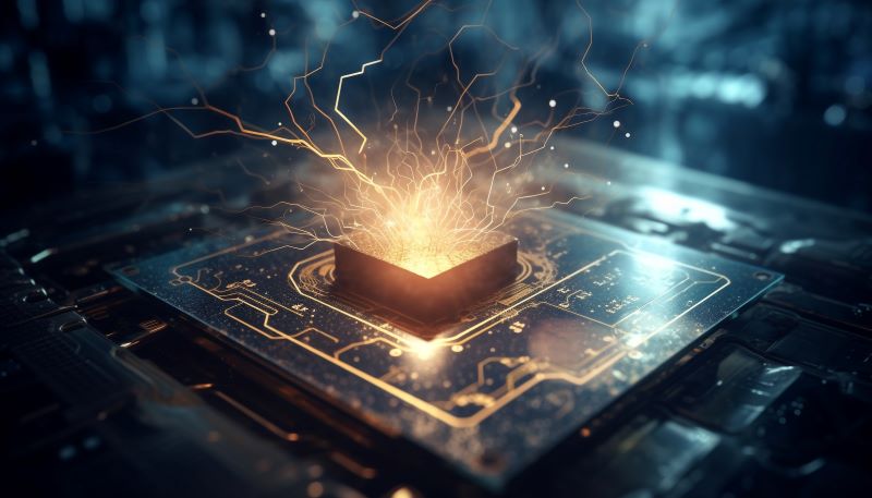
Part 2: What not to forget when manufacturing high frequency printed circuit boards – Electrical Signals and Electromagnetic Interference
Minimizing and Eliminating Electromagnetic Interference in PCBs:
- Proper PCB Design: During PCB design, it is important to consider the placement of components, traces, ground planes, and PCB layers. Proper component and trace placement can minimize crosstalk and interference between signals.
- Ground Planes and Layers: Ground planes and layers serve to dissipate interference and provide a path for electromagnetic energy. Proper distribution of ground planes and layers can help minimize interference.
- Component Placement: Components should be placed in a way that minimizes interference between them. For example, sensitive analog circuits should be isolated from disruptive digital circuits.
- Trace Routing: Traces should be routed to minimize crosstalk and interference. Shielding of traces can also be employed to minimize the emission of disruptive signals.
- Use of Decoupling Capacitors and Filters: Decoupling capacitors and filters can help eliminate or minimize high-frequency noise and interference.
- Proper Grounding Practices: Proper grounding practices, including the correct connection of ground planes and layers, can help minimize ground loops and interference. A ground loop occurs when there are multiple paths for current flow in an electrical circuit. It occurs when different grounding points are interconnected or connected in the circuit. This loop can create unwanted currents and induce electromagnetic interference.
- Use of Shielded Enclosures: In some cases, it may be appropriate to use shielded enclosures or shields to protect against external electromagnetic interference.
It is also important to utilize advanced PCB design software tools that provide options for EMI analysis, crosstalk simulations, and other EMI-related aspects.
Specific examples of eliminating electromagnetic interference (EMI) in PCBs for high-frequency applications.
Proper material selection for PCBs has a significant impact on EMI. For example, choosing a material with a low loss tangent (tan δ) minimizes signal losses and overall high-frequency interference.
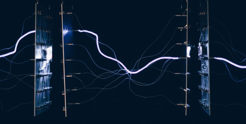
The use of differential signal traces in PCBs also helps. Differential signal traces are used for data transmission between electronic components on the PCB. These traces consist of two conductors (a pair) with opposite polarity, carrying signals between components on the PCB. EMI affects both conductors of the pair in the same way. However, the differential receiver circuit analyzes only the differences between them, effectively canceling out interference in the resulting signal. By equalizing the signal in the pair of differential conductors, these traces are less susceptible to noise that may occur along the signal path. This means that differential traces can transmit signals over longer distances or in environments with higher interference without degrading signal quality.
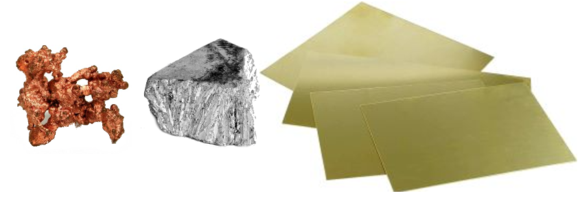
High-quality connectors for proper signal transmission and interference minimization must meet several key characteristics, such as low impedance (minimizing resistance and inductance in the signal path). Connectors should be made of materials with good EMI resistance, such as metals like brass, aluminum, stainless steel, ferrite, or ferrite ceramics, which typically have good conductivity and the ability to reflect electromagnetic waves.
The lowest electrical resistivity, which is a physical property of a material indicating its ability to resist the flow of electric current, is typically exhibited by the alloy of copper and zinc, namely brass.
- It is also important to note that if signal traces encounter bends or crossings of high-frequency paths, they can create large loops and become sensitive to external noise.
- Another rule is to minimize parallel crosstalk between output and input traces over long distances. These crosstalks can cause signal interference, but they can be reduced by adding ground planes or increasing the distance between traces.
- We must not forget that bending traces at a 90° angle causes signal losses. This type of bending creates disruptive reflections and degrades signal properties. Instead, it is recommended to use curved shapes or angles around 45°, which minimize interference and maintain signal integrity.
- A crucial rule for signal traces is to keep them as short as possible. Shorter signal traces reduce the path of coupling disruptive signals. It is recommended to route important signal traces, such as clock signals and sensitive data lines, first. High-speed signal traces should follow, with less significant signal traces being routed last.
Adhering to these rules and techniques can significantly contribute to reducing electromagnetic interference and voltage spikes in high-frequency PCBs. High-quality design and the correct use of suitable materials and techniques can lead to reliable and efficient operation of these boards in various high-frequency applications.
Signal Interference and Electrostatic Discharges
Electrostatic discharges (ESD) need to be taken into account in the design and production of high-frequency printed circuit boards (PCBs). High-frequency applications present a specific challenge because high-frequency signals are susceptible to various forms of interference, and electrostatic discharge can cause damage to sensitive components.
Signal interference can originate from various sources, including electromagnetic radiation from neighboring devices, voltage surges in power networks, or inherent electromagnetic interference within the board itself. This can lead to signal degradation, distortion, and even system failure. To minimize interference, it is important to adhere to proper trace and conductor geometry on the PCB. Too-close parallel routing can lead to cross-talk interference, while improper trace placement can result in unwanted resonances and oscillations on the PCB.
Static electric discharge occurs during the handling of electronic components or when connecting and disconnecting connectors. ESD can cause damage to sensitive components and reduce their reliability. Protective circuits, such as Transient Voltage Suppression (TVS) diodes, are used to protect against electrostatic discharges. These diodes absorb excess energy during discharge, thereby protecting sensitive components from damage.
- Voltage surges occur on PCBs when the voltage exceeds the permissible level required for proper operation of electronic components on the board.
- Instability or transient events in the power supply system, such as voltage surges or interference, can lead to voltage surges on the PCB.
- During signal transmission between different devices, interference and voltage surges can occur due to poor quality or noisy signal lines. Voltage surges can affect electronic components connected to these lines.
Capturing all the important aspects of signal interference and ESD in high-frequency PCBs requires a careful approach and expertise in the field. Thorough design, proper manufacturing practices, and the use of suitable protective measures are key to achieving high quality, reliability, and performance in high-frequency PCBs.
Voltage surges can cause serious problems, including component damage, signal disturbances, and even complete system failure. Therefore, it is important to use measures and components that minimize the risk of voltage surges on PCBs.
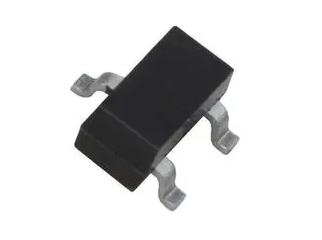
One measure that can be used is the utilization of Schottky diodes. Schottky diode is a special type of diode that has a low forward voltage drop and a fast response. This diode is typically made with a metal contact on a semiconductor material and has the ability to quickly respond to voltage changes.
Schottky diodes were invented by engineer and physicist Léon Charles Schottky, who was from France and developed them in collaboration with Siemens around 1938.
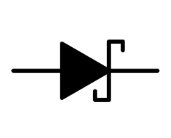
- Schottky diodes are often used for overvoltage protection in electronic circuits, including PCBs. By connecting a Schottky diode in parallel with protected signal lines, their influence on surrounding circuits can be limited. During a voltage surge, the Schottky diode rapidly responds and dissipates excess energy to the ground, thereby protecting other components on the board from damage.
- It is important to carefully select the appropriate Schottky diode for a specific application. When choosing a diode, factors such as maximum current, maximum voltage, and response speed needed for the system should be considered. High-quality Schottky diodes have low capacitance and low impedance, allowing them to effectively limit voltage surges.
- However, Schottky diodes are not the only solution for overvoltage protection. Other measures and components, such as transient voltage suppression (TVS) diodes, varistors, polyfuses, proper component and power circuit placement, and proper grounding techniques, should also be considered based on the specific needs and requirements of the system.
- Overall, overvoltage protection in PCBs is an important aspect of design and manufacturing. The use of Schottky diodes and other appropriate measures can significantly reduce the risk of voltage surges and ensure reliable operation of the PCB. However, it is important to carefully consider specific requirements and make the right choice of components and measures to ensure the best protection and performance of the PCB.
When manufacturing high-frequency PCBs, it is crucial to collaborate with experts who have experience in high-frequency applications. The use of proper materials, design optimization, and utilization of modern technologies can significantly contribute to minimizing EMI and overvoltage in high-frequency PCBs. Additionally, consideration should be given to other physical properties we introduced in the first part: What to Watch Out for When Manufacturing PCBs for Extreme Environments?
Expert knowledge, experience, and collaboration with a professional PCB manufacturer are crucial for successfully addressing these challenges and achieving high quality and reliability in high-frequency PCBs.
Connect with our specialists