Economics of development and production of electronic devices - Volume 2
Electrical diagram design
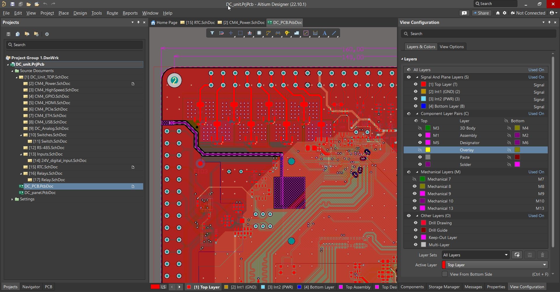
If you have decided to implement an electronic product based on the results of the analysis, the first stage of development will be the design of the electrical schematic. Use one of the
one of the proven ECAD systems such as Altium Designer, OrCAD PCB Designer, PADS, Xpedition, Fusion 360 (Eagle) or freeware KiCAD.
Choosing the right ECAD system
The choice of ECAD system depends primarily on the resources available and the frequency with which you will use the system. The choice of the appropriate system also depends on the complexity of the designs you will be creating.
In general, you can design a multilayer board with signals up to about 100 MHz
with varying degrees of effort in any available professional or semi-professional system. Premium systems such as Altium, OrCAD or Xpedition provide users with features that make design easier and more straightforward in many ways. For more complex designs, they are the obvious choice.
What are the benefits of premium systems? An excellent example is the support for the design of impedance-controlled connections and differential pairs. If the system in use does not offer such support, designing a board with differential pairs will certainly be more complicated, and therefore more expensive, than a system that does support differential pair design.
We have written many times in the past about the features and selection of a suitable ECAD system (e.g. here), so we will not go into them in detail now.
Selection of suitable components
We have relative design freedom when designing a schematic. Nevertheless, we have to respect a number of constraints, which are determined by the functional characteristics defined in the analysis, the electrical and mechanical concept, the manufacturing cost calculation and, last but not least, the short – and long-term availability of components in distribution.
If the device is to operate over a wide operating temperature range from -40 °C to +70 °C according to the functional characteristics, then suitable components must be selected to meet this condition. The same applies to parameters such as operating voltage, power dissipation, life expectancy, etc. These parameters must be met, so there is little room for compromise.
If we want to achieve manufacturing cost savings when selecting components, or are constrained by the end price of the product, we can only achieve this by selecting the appropriate manufacturer and distributor for each component and negotiating quantity or project discounts where appropriate. However, we should never discount the requirements embodied in the functional characteristics and project analysis.
Check availability of components
For each individual component we have to check the current availability for prototyping. We only select components that can be expected to be available after the product development is complete and mass production has started.
Due to the current shortage of parts on the market and long lead times, parts are secured well in advance for repeat production. Sometimes they are purchased as soon as the prototype has been verified, sometimes as part of the purchase of components for prototype production.
Select parts with compatible replacements
One effective method to reduce the risk of component unavailability is to select components
with available replacements. These are components for which a fully compatible and functional replacement exists in the form of an alternative component from the same (or even a different) manufacturer. A fully compatible replacement is a component that not only has the same electrical characteristics as the component being replaced, but also has the same housing and can be fitted in place of the component being replaced without PCB modification.
In some cases, however, you may need to use components that are not fully compatible replacements. Typically these are switching power supplies, microprocessors, Ethernet controllers, special analog circuits or special digital peripherals. In this case, the only solution is to address availability by purchasing the required quantity of components in stock in a timely manner.
Mounting method
Another consideration when selecting electronic components is how they are assembled. Currently, surface mount printed circuit board (SMD) components are most commonly used. Their main advantage is the possibility of automatic machine assembly, which is cheaper, faster and more reliable compared to manual assembly.
Where possible and appropriate, we recommend that SMD components are always preferred. Only in cases where there is no suitable SMD alternative, or where it is not possible to use an SMD component for mechanical reasons, should pin type (THT) components be used.
Even with pin components, you can avoid manual fitting if you use automatic selective soldering of pin components. A prerequisite for selective soldering, however, is a suitable PCB design, where a protection zone without SMD components must be maintained around the THT pads on the soldered side. In general, the use of SMD and THT components has its specifics in terms of manufacturability, which must be respected in the design. Failure to follow the design rules or to respect the technical conditions of the assembler may result in a higher price for the PCB assembly.
Surface joint – determination of materials and layers
With the appropriate electronic components selected, we can now turn our attention to the PCB itself. First of all we have to select the base material and determine the number of layers and their composition.
Materials
For the purposes of this article, we will be looking at solid PCBs, the base material of which is in most cases a glass fibre composite bonded with epoxy resin. In practice, however, you may also encounter less frequently used materials such as ceramic-filled RF materials, power substrates with metal core (IMS) or flexible PCBs.
Generally, a PCB is made by laminating several layers of base (non-conductive) material and copper sheets. When selecting the base material, we base our selection on the functional characteristics and are primarily interested in the following parameters:
- operating temperature range,
- the requirement for non-flammability or flame retardancy of the material,
- frequency of signals,
- the requirement for controlled impedance.
Nowadays, PCB manufacturers are exclusively using high quality materials that have a stable dielectric constant DK (i.e. we can implement connections with controlled impedance up to frequencies of approx. 100 MHz), a high delamination point (Tg > 120 °C) and are self-extinguishing, which is suitable for most applications.
In the case of developing simple low frequency devices, we can reach for standard stock material for double-sided or multilayer PCBs. On the other hand, if we need to implement impedance controlled connections for frequencies above 500 MHz, we need to choose more expensive high frequency material. High-frequency materials differ from low-frequency ones mainly in their higher fibre density, which results in a more stable dielectric constant DK over the whole area.
What else affects the price of a PCB
Other parameters that affect the price of a PCB include the number of layers, the design class or the use of superior technologies. This is where we most often encounter price optimization efforts, which, however, can ultimately have both a negative impact on the performance of the device and a significant impact on the overall project economics.
Number of layers
In general, double-sided PCB is suitable for the simplest low-frequency devices. For these devices, not only signal connections but also a sufficiently compact distribution of supply voltages and grounds can be realized on two layers.
If the device contains a switching power supply or processor or impedance controlled connections, or is a mixed digital and analogue design, we strongly recommend the use of a 4layer PCB.
You can use the outer layers for the connections and the inner layers for the printed wiring of the supply voltages and grounds. This PCB configuration provides enhanced RF signal quality, reduces emissions and also increases immunity to electromagnetic interference. There is also a significant saving in design time when the designer does not have to complexly create power and ground connections between other signals. Conversely, when trying to design such a device on a double-sided PCB, even with significantly longer design time, the device may not meet the functional requirements or operate reliably. The more complex the electrical circuitry then becomes, the greater the requirement for the number of layers and their composition.
Choice of design class
The complexity of the design is also related to the choice of the design class. The design class determines the minimum joint and gap width for a given copper plate thickness and also the minimum width of the drilled hole annulus. The more components with high integration and the more joints there are on the board, the higher the design class, and therefore the thinner the joints, should be used.
Again, the cost optimisation of using a lower design class (wider junctions and gaps) than the design requires may result in greater design difficulty or possibly inability to maintain isolation distances between groups of high frequency signals, etc. Conversely, the use of a higher design class than is strictly necessary may lead to unnecessary cost overruns on the PCB.
Execution of punched holes
Other PCB characteristics that we need to take into account include the design of the punched holes (standard, filled, reflowed, buried, use of microvia), masks, prints, surface treatments, etc. It is always the case that the use of standard or superior technologies must be carefully considered with regard not only to cost, but also to the functional characteristics of the product and the subsequent manufacturing processes.
If, for example, we use components with low pad spacing in the design or use BGA-type housings, it is advisable to ensure that the resulting PCB surface is as flat as possible. This is especially true if reflow soldering is performed. In this case, the standard HAL surface treatment, which is created by immersing the PCB in a bath of molten tin solder, does not produce a sufficiently flat surface. To ensure maximum surface flatness, we therefore choose the additional service of immersion or electroplating.
However, in the case of vapour brazing, the most suitable surface finish for the PCB is HAL. Immersion gold plating, on the other hand, appears to be the least suitable for this soldering technology. If, for example, we need to use cooling vias located directly in the pads of power components, we must consider filling and reflowing the vias, which may otherwise leak tin. The joint may then not be of sufficient quality.
Summary
The above examples of PCB parameters and properties are far from complete. PCBs are so complex that a detailed description of their properties would take a whole book. In this article, we wanted to draw attention in particular to the aspects that must be taken into account when designing PCBs.
In the article, we have summarized the general rules in the selection of components and in the choice of PCB parameters, which have a clear impact on the economics of the project. In the final part of the article on the economics of the development and production of electronic devices, we will focus on the production of the prototype, its testing and finally the launch of the product on the market.
Connect with our specialists